_1673427121.png)
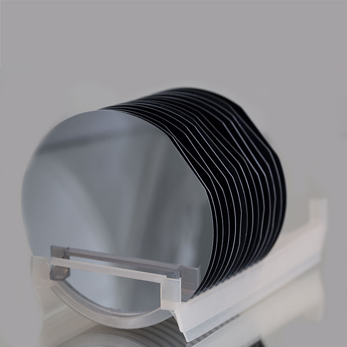
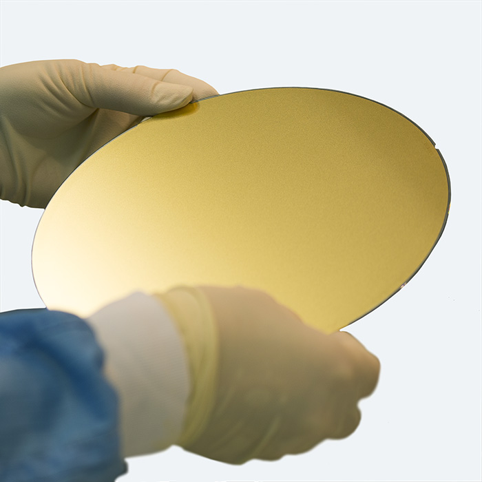
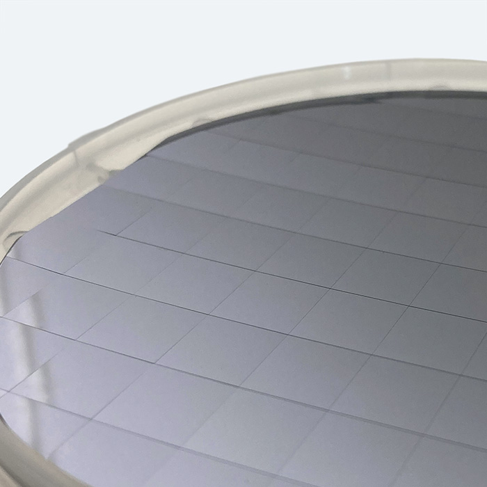
Silicon wafers
Download PDF documentationInformation guide
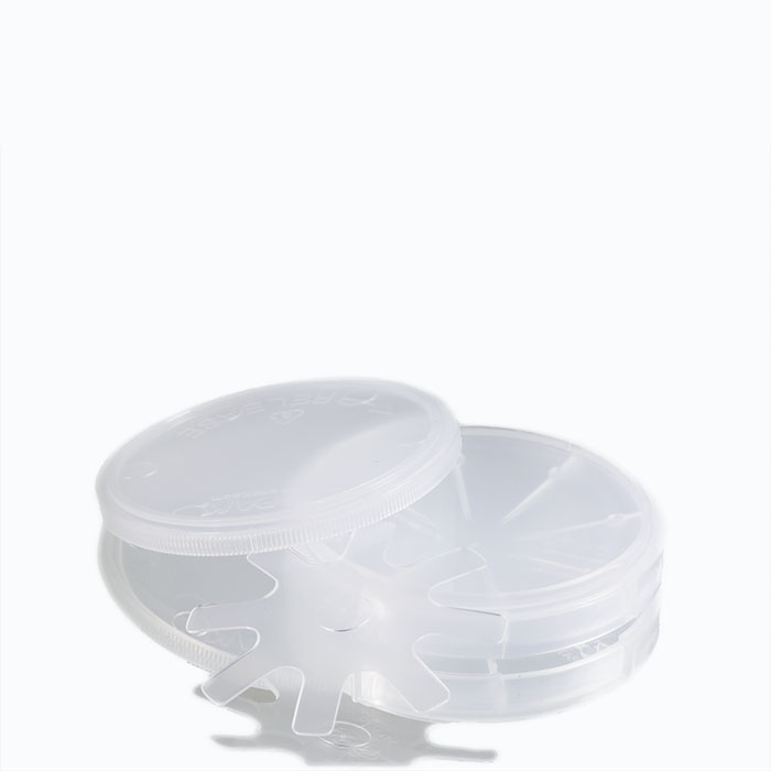
Silicon wafers :
Silicon wafers are cut from Silicon single crystal using internal diameter diamond discs. They are used for production of silicon substrates and membranes.
The below mentioned parameters are dealing with our standard products.
On the customer's request we are ready to discuss orders for wafers with some other parameters. All of our silicon wafers are delivered with certificate of analysis.
Direct link to the wafers tweezers page : tweezers
Metallurgical-Grade Silicon Production :
Quartz sand is reduced with carbon in an electric arc furnace at temperatures > 1900°C to metallurgical grade silicon (> 98 % pure). The major part of the world production (2008: approx. 6 million tons) is used for manufacturing alloys with aluminium and steel, and as raw material for polysiloxane production.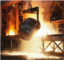
In 2010, Si wafer production consumed approx. 200 kilotons purified silicon. Approx. 90 % of this volume was used for mono- and polycrystalline solar cells, the remaining 10 % (corresponding to a wafer area of » 5 km2) went into the semiconductor industry.
Purification of Silicon
The impurity concentration in metallurgical-grade silicon is many orders of magnitude too high for an application in photovoltaics and microelectronics, thus the silicon has to be purified. For this reason, silicon intended for wafer production is converted into trichlorosilane gas (HSiCl3) at » 300°C using hydrochloric acid via
Si + 3 HCl à HSiCl3 + H2
which already removes many impurities which don’t form volatile chlorine compounds at the applied process temperature.
Trichlorosilane (boiling point 32°C) mixed with other gaseous chlorine compounds undergoes multiple distillation thereby improving the purity up to 99,9999999 %. („9N“) and is subsequently thermally decomposed to polycrystalline silicon.
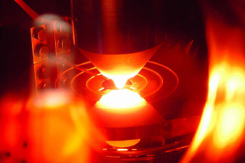
The polycrystalline silicon formation is performed in the so-called Siemens-Process (fig. right): The purified trichlorosilane mixed in hydrogen is thermally decomposed on the surface of a heated (approx. 1100°C) silicon rod via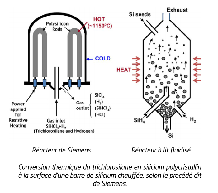
HSiCl3 + H2 à Si + 3 HCl
to polycrystalline silicon and HCl, which corresponds to the reverse reaction of the trichlorosilane formation. This “electronic-grade“ (purity concentration <1014 cm-3) polysilicon is the raw material for silicon single crystals which are grown by two different processes as described in the following sections.
Growth Techniques for Monocrystalline Silicon Ingots
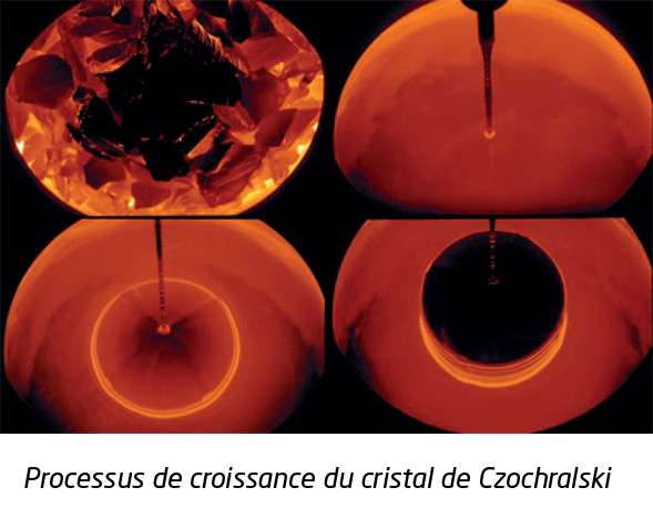
Czochralski-Technique
Basics
The Czochralski-technique is a method to pull a monocrystal with the same crystallographic orientation of a small monocrystalline seed crystal out of melted silicon. First, electronic-grade polysilicon nuggets (e. g. from the Siemens-process) optionally together with dopants are melted in a quartz crucible at a temperature > 1400°C in an inert gas atmosphere (e. g. argon). The quartz crucible sits inside a graphite container which – due to its high heat conductivity – homogeneously transfers the heat from the surrounding heater to the quartz crucible.
The silicon melt temperature is kept constant roughly above the silicon melting point. A monocrystalline silicon seed crystal with the desired crystal orientation (e. g. <100>, <110> or <111>) is immersed into the melt and acts as a starting point for the crystal formation supported by the heat transfer from the melt to the already grown crystal.
The seed crystal is slowly (few cm/hour) pulled out of the melt, where the pull speed determines the crystal diameter. During crystal growth, the crystal as well as the crucible counter-rotate in order to improve the homogeneity of the crystal and its dopant concentration.
Before the crystal growth is finished, a continuous increase of the pull speed reduces the crystal diameter towards zero. This helps prevent thermal stress in the ingot which could happen by an abrupt lifting out of the melt and could destroy the crystal.
Advantages and Disadvantages
The Czochralski-technique allows big crystal diameters (state of the art: 18 inch = 46 cm) and – compared to the float-zone technique described in the following section – lower production cost per wafer.
One disadvantage of the Czochralski-technique is impurities such as oxygen (typ. 1018 cm-3) and carbon (typ. 1017 cm-3) from the quartz and graphite crucible which lower the minority carrier diffusion length in the finished silicon wafer.
Another disadvantage is a comparably low homogeneity of the axial and radial dopant concentration in the crystal caused by oscillations in the melt during crystal growth. This makes it difficult to attain high-ohmic CZ-wafers with a resistivity exceeding» 100 Ohm cm). A magnetic field (“Magnetic Czochralski”, MCZ) can retard these oscillations and improve the dopant homogeneity in the ingot.
Float-Zone Technique :
A monocrystalline silicon seed crystal is brought into contact with one end of a polycrystalline silicon ingot. Starting from here, an RF coil melts a small region of the polysilicon which, after cooling down, forms monocrystalline silicon with the crystallographic orientation of the seed crystal (e. g. <100>, <110> or <111>).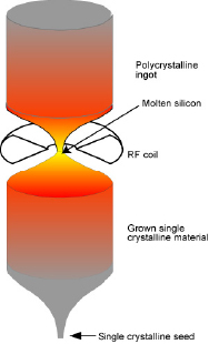
The RF coil and the melted zone move along the entire ingot. Since most impurities are less soluble in the crystal than in the melted silicon, the molten zone carries the impurities away with it. The impurities concentrate near the end of the crystal where finally they can simply be cut away. This procedure can be repeated one or more times in order to further reduce the remaining impurity concentration.
Doping is realized during crystal growth by adding dopant gases such as phosphine (PH3), arsine (AsH3) or diborane (B2H6) to the inert gas atmosphere.
Advantages and Disadvantages
The main advantage of the float-zone technique is the very low impurity concentration in the silicon crystal. In particular the oxygen and carbon concentration are much lower as compared to CZ silicon, since the melt does not come into contact with a quartz crucible, and no hot graphite container is used.
Additionally, the dopant concentration in the final crystal is rather homogeneous and manageable which allows very high-ohmic (1 - 10 KOhm cm) wafers as well as wafers with a narrow specified electrical resistivity.
However, FZ silicon is more expensive than CZ silicon, and the crystal diameter is limited to eight inches (state of the art).